Image Processing in High Resolution Electron Microscopy

References:
[1] Z.H. Wang, Y.D. Liu, Z.Q. Fu, Y. Li, T.Z. Cheng,
F.H. Li & H.F. Fan, "Visual computing in electron crystallography" Z. Krist.
218, 308-315 (2003)

Background
For the structure analysis
of crystalline materials, electron crystallographic methods are in some
cases superior to that of X-rays. Firstly, many crystalline materials important
in science and technology, such as high Tc superconductors, are too small
in grain size and too imperfect in periodicity for an X-ray single crystal
analysis to be carried out, but they are suitable for electron microscopic
observation. Secondly, the atomic scattering factors for electrons differ
greatly from those for X-rays and, it is easier for electron diffraction
to observe light atoms in the presence of much heavier atoms. Finally the
electron microscope is the only instrument that can simultaneously produce,
for a crystalline sample, a microscopic image and a diffraction pattern
at atomic resolution. In principle either the electron micrograph (EM)
or the electron diffraction (ED) pattern could lead to a structure image.
However the combination of the two will make the procedure much more efficient
and powerful.
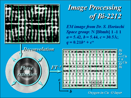
There are two difficulties
in using electron microscopic methods in solving crystal structures. Firstly,
an electron microscope image is not a true structure image of the object
but just a convolution of the true image with the Fourier transform of
the contrast transfer function. Secondly, the point to point resolution
of an electron microscope image is not enough to reveal individual atoms
in most cases. Hence it is essential to have some technique for both image
deconvolution and resolution enhancement. A two-stage image processing
procedure making use of direct methods has been developed, which combines
information from an electron microscope image and the corresponding electron
diffraction pattern.